
In this tutorial we cover the following topics
The 555 is probably the most versatile chip that exists, with endless applications. Its relatively powerful output (rated at up to 200mA) is extremely useful, and the chip itself is hard to damage. Invented in 1970 it is still in use and there is no premises that this situation will change in forseable future.

|
In some sense, the 555 itself is unable to do anything constructive -- it has to be accompanied by other elements, chips or circuits. Generally speaking 555 is a timing system. These devices are precision timing circuits capable of producing accurate time delays or oscillation. Contrary to appearances, its universality is the result of simplicity. In the structure of this chip, we distinguish only five blocks that can be configured in various ways.
For the 555 to function it relies on both analogue and digital electronic techniques, but if we consider its output only, it can be thought of as a digital device. The output can be in one of two states at any time, the first state is the LOW state, which is 0V. The second state is the HIGH state, which is the voltage of our power supply. The most common types of outputs can be categorized by the following
- Monostable mode In this mode, the 555 functions as a "one-shot" or "push to operate" circuit.
This type of circuit produces one pulse of a defined length in response to a trigger input such as a push button. The output of the circuit stays in the low state until there is a trigger input, hence the name "monostable" meaning "one stable state". Next for a predefined time output switch to high state and after that goes to low until another "impuls". It can be used for an automatic light off. We can push a button to turn light on, and the circuit will automatically switch it off after a predefined time.

- Bistable The 555 can operate as a flip-flop.
In this mode we have two stable states, high and low. Taking the triggerTRIGinput low makes the output of the circuit go into the high state. Taking the resetRESETinput low makes the output of the circuit go into the low state. This type of circuit is ideal for use in an automated go-and-back models used for example with railway system where the train is required to run back and forth over the same piece of track.

- Astable The 555 can operate as an oscillator.
In this mode, ther is no stable state -- hence the name "astable". The output continually switches state between high and low without any intervention from the user. This type of circuit could be used to flash lamps and LEDs, and is useful as a "clock" pulse for other digital ICs and circuits.

The 555 chip has only eight pins (see xx555 Precision Timers documentation or its ne555.pdf ![]() )
)

|
- Pin 1
GNDGround. - Pin 2
TRIGStart of timing. - Pin 3
OUTOutput signal. When output is active it switch toHIGHstate. - Pin 4
RESETReset timer.LOWstate on this pin forces output to switch toLOWstate. - Pin 5
CONTControls internal comparator thresholds. - Pin 6
THRESEnd of timing input (whenTHRES>CONT). - Pin 7
DISCHTechnically speaking: open collector output to discharge timing capacitor. - Pin 8
VCCInput supply voltage, in most cases from 5V to 15V.
Please notice, that in a circuit diagram the 555 timer chip is often drawn like the illustration below. The pins are not in the same order as the actual chip, this is because it is much easier to recognize the function of each pin, and makes drawing circuit diagrams much easier.

|
As it was mentioned earlier, inside the 555 chip, we distinguish only five blocks. Describing them we will use a simplified schematic diagram

|
- Voltage divider

Three resistors with the same values (typically 5kOhm -- now it's clear why this chip has 555 as its name) create the voltage divider. They divide the supply voltage applied between the pin 8 (VCC) and 1 (GND) into three equal parts. - Voltage comparators.
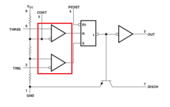
Voltage comparators. - SR flip-flop
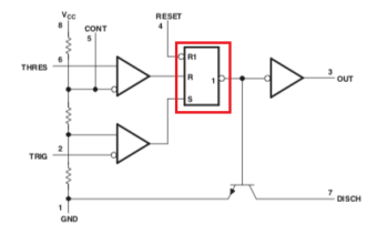
In electronics, a flip-flop or latch is a circuit that has two stable states and can be used to store state information. The circuit can be made to change state by signals applied to one or more control inputs and will have one or two outputs. It is the basic storage element in sequential logic. Flip-flops and latches are fundamental building blocks of digital electronics systems used in computers, communications, and many other types of systems. All flip-flops can be divided into common types: the SR ("set-reset"), D ("data" or "delay"), T ("toggle"), and JK.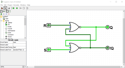

Left image: S=1,R=0to setQ. Right image:S=0,R=0preserve previous state.
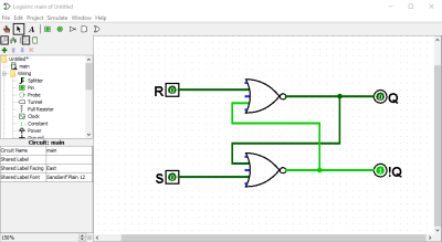
Left image: S=0,R=1to resetQ. Right image:S=0,R=0preserve previous state.In case of SR, while the
RandSinputs are bothLOW, feedback maintains theQand!Qoutputs in a constant state, withQthe complement of!Q. IfSis pulsedHIGHwhileRis heldLOW, then theQoutput is forcedHIGH, and stays high whenSreturns toLOW; similarly, ifRis pulsedHIGHwhileSis heldLOW, then theQoutput is forcedLOW, and staysLOWwhenRreturns toLOW.The
R = S = 1combination is called a restricted combination or a forbidden state because, it breaks the logical equationQ = !Q(which is a consequence of internal structure, where two NOR gates are used).In 555 chip SR flip-flop is used to remember the output states of voltage comparators.
The functions of its oins are as follows:- S -- set -- high state set
Qoutput to high state, - R -- reset -- high state sets
Qoutput to low state, - !R1 -- master reset -- low state turns off
Qoutput regardless of the state of the other two inputs, - Q -- flip-flop output,
- !Q -- negated output of the flip-flop (opposite to
Q).
- S -- set -- high state set
- Output buffer

Between theQoutput of the SR flip-flop and the output OUT of the circuit there is an output buffer, whose task is to increase the current efficiency of this output. Thanks to it, diodes or relays can be connected directly to the 555 output. - Discharge transistor
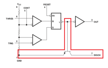
This transistor has a special function: it discharges the external capacitor.


- The NE555 chip is very cheap to produce.
- We can easily configure it in different ways, with just a several passive elements.
- The times of generated pulses do not depend on the supply voltage.
- High current consumption.
- Extended first impulse in relation to the others. This is due to the need to charge the capacitor from zero, while later it is discharged to 1/3 of the supply voltage.
- The NE555 is not suitable for precise measuring of very long times.
- On the other side, we can obtain only 500kHz or slightly more.
As it was explained in the Introduction section in monostable mode, also known as one-shot mode, the timer delivers only one pulse in response to a triggering event. A transition to
LOW voltage on the trigger pin TRIG creates a HIGH pulse from the output pin OUT. The duration of the pulse is determined by the value of resistor R and capacitor C, as the resistor charges the capacitor. If the reset pin RES of the timer will not be used, it should be connected the positive side of the power supply to prevent it from being activated unintentionally; low voltage on this pin resets the timer. Second capacitor 0.1nF connected to control CONT pin suppress noise.

|

|
| Typical connections of a 555 timer in monostable mode | |

|
| Output signal in monostable mode |
Below a table with pulse duration dependence (in seconds) on resistance and capacity combination are given
| R=10kO | R=22kO | R=33kO | R=47kO | R=100kO | R=220kO | R=330kO | R=470kO | R=1MO | |
| C=0.01uF | C=0.022uF | ||||||||
| C=0.1uF | 0.11 | C=0.22uF | |||||||
| C=1uF | 1.1 | C=2.2uF | |||||||
| C=10uF | 1.1 | 2.4 | 5.2 | 11 | C=22uF | ||||
| C=100uF | C=220uF |
If we want a pulse duration differnt then are given in a table, we can use a simple formula,
$$T = R \cdot C \cdot 0.0011$$
where
- $T$ is the pulse time in seconds,
- $R$ is the resistance in kilohms,
- and $C$ is the capacitance is microfarads.
Doing this, bear in mind that
- Resistor values below 1k should not be used.
- Resistor values below 10k are undesirable, as they increase power consumption.
- Capacitor values above 100uF may produce inaccurate results because leakage in the capacitor becomes comparable with its charging rate.
- The result we obtain may not be exact (as given by formula), because resistor and capacitor values in most cases are inaccurate (we have some tollerance). There are also many other factors such as ambient temperature which may affect final timing.
To test this circuit we may want use LEDs. A god explanation how to do this (how to choose LED and resistor for them) without breaking them we may find in
- Jak dobrać rezystor do diody? Różne metody zasilania LED! (in polish)
- LEDs for Beginners (in english)
We may use the following circuit
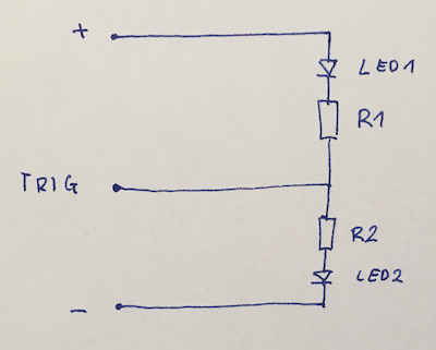
As a rule of thumb we should remember to use the following formula to figure out which resistor to use
$$
R = \frac{V_{power} - V_{LED}}{I_{LED}}
$$
where
- $V_{power}$ -- power supply voltage,
- $V_{LED}$ -- LED voltage,
- $I_{LED}$ -- LED current (usually 20mA).
Some examples of calculations:
0.02A = 20mA = 20 * 0.001A
0.01A = 10mA = 10 * 0.001A
(5-2)/0.02 = 150 Ohms
(5-2.25)/0.02 = 137.5 Ohms
(5-3)/0.02 = 100 Ohms
(5-2)/0.01 = 300 Ohms
(5-2.25)/0.01 = 275 Ohms
(5-3)/0.01 = 200 Ohms
(3.3-2)/0.02 = 65 Ohms
(3.3-2.25)/0.02 = 52.5 Ohms
(3.3-3)/0.02 = 15 Ohms
(3.3-2)/0.01 = 130 Ohms
(3.3-2.25)/0.01 = 105 Ohms
(3.3-3)/0.01 = 30 Ohms

|

|
C=10uF, R=470kO |
|
monostable_film.mov

|

|
| Typical connections of a 555 timer in bistable mode | |

|
| Output signal in bistable mode |

|

|

|
| Typical connections of a 555 timer in astable mode | |

|
| Output signal in astable mode |
As we can see, in this mode output changes endlessly its state from HIGH to LOW and next from LOW to HIGH. How do the values for the timing capacitor and the resistors determine the frequency (frequency = high state time + low state time) of the timer? If R1 and R2 are measured in kilohms, and C is measured in microfarads, the frequency f, in hertz, is given by:
$$
f = \frac{1.440}{ ( ( 2 \cdot R2 ) + R1 ) \cdot C }
$$
In the table below some values are given.
| R1 | R2 | C | f | High state (s) | Low state (s) |
|---|---|---|---|---|---|
| 10kO | 10kO | 47uF | 1.023 | 0.651 | 0.325 |
| 10kO | 10kO | 4.7uF | 10.234 | 0.065 | 0.032 |
| 10kO | 47kO | 4.7uF | 2.952 | 0.185 | 0.153 |
| 10kO | 100kO | 4.7uF | 1.462 | 0.358 | 0.325 |
| 100kO | 100kO | 4.7uF | 1.023 | 0.651 | 0.325 |
| 100kO | 100kO | 47uF | 0.102 | 6.514 | 3.257 |
| 47kO | 47kO | 47uF | 0.218 | 3.062 | 1.531 |
| 50kO | 50kO | 47uF | 0.205 | 3.257 | 1.629 |
For other combinations you can use 555 Astable Circuit Calculator.

|

|
R1=R2=10kO, R=330O, C1=100nF = 0.1uF, C2=47uF |
|

|

|
R1=R2=50kO, R=330O, C1=100nF = 0.1uF, C2=47uF |
|
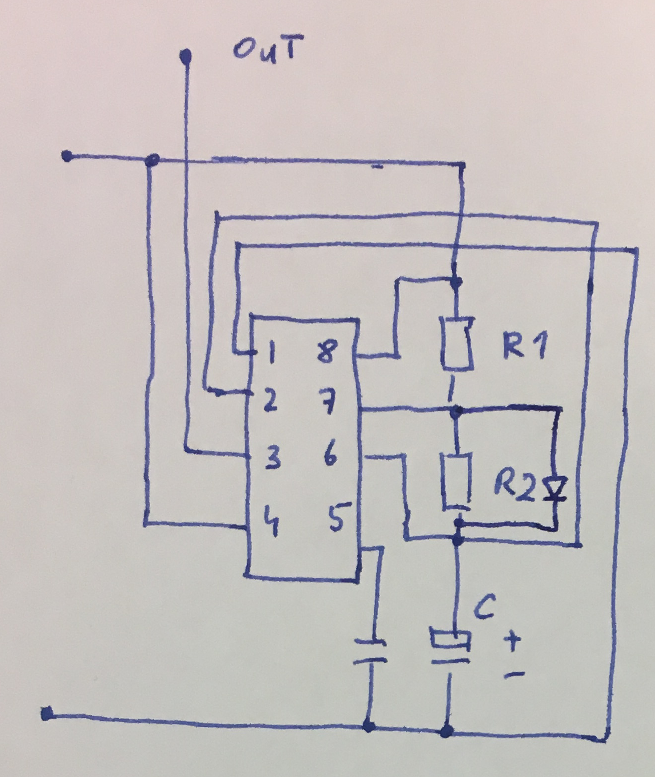
When the 555 chip is wired in the standard way for astable mode, high pulses are always longer than gaps between them in the output. Explanaiton of this is quite simple.
When the timer is running in astable mode, C charges through R1 and R2 in series. But when C discharges, it dumps its voltage into the chip through R2 only. Because the capacitor charges through two resistors but discharges through only one of them, it charges more slowly than it discharges. While it is charging, the output on pin 3 is HIGH; while it is discharging, the output on pin 3 is LOW. Consequently the on state is always longer than the off state.
If we want the on and off cycles to be equal, or if we want to adjust the on and off cycles independently (for example, because we want to send a very brief pulse to another chip, followed by a longer gap until the next pulse), all we need to do is add a diode, as shown below

|
|
| Connections of a 555 timer in on-off equal astable modee | |
Adding a diode to bypass R2 allows the high and low output cycles of a timer to be adjusted independently. Now when C charges, the electricity flows through R1 as before but takes a shortcut around R2, through the diode (because a diode deducts some voltage, this circuit works best with a supply voltage greater than 5V). When C discharges, the diode blocks the flow of electricity in that direction, and so the discharge goes back through R2. R1 now controls the charge time on its own, while R2 controls the discharge time. The formula for calculating the frequency is now approximately
$$
f = \frac{1.440}{( R1 + R2 ) \cdot C }
$$
where R1 and R2 are in kilohms and C is in microfarads. If we set R1 = R2, we should get almost equal on/off cycles.