
Published: 2022-01-03
Last update: 2023-06-30
In this tutorial you will learn what to do if the number of available pins you have at your disposal is not enough to connect everything you want your system to interact with.
Table of contents
Although most of microcontrollers have many input/output pins, there are no problems to spend all of them and find yourselves in a situation when there would be no option to attach anything else. In this part I will show what you can do in case of such a situation. Other words, I will show how to "multiply" your pins.
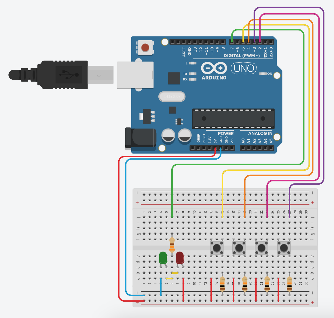
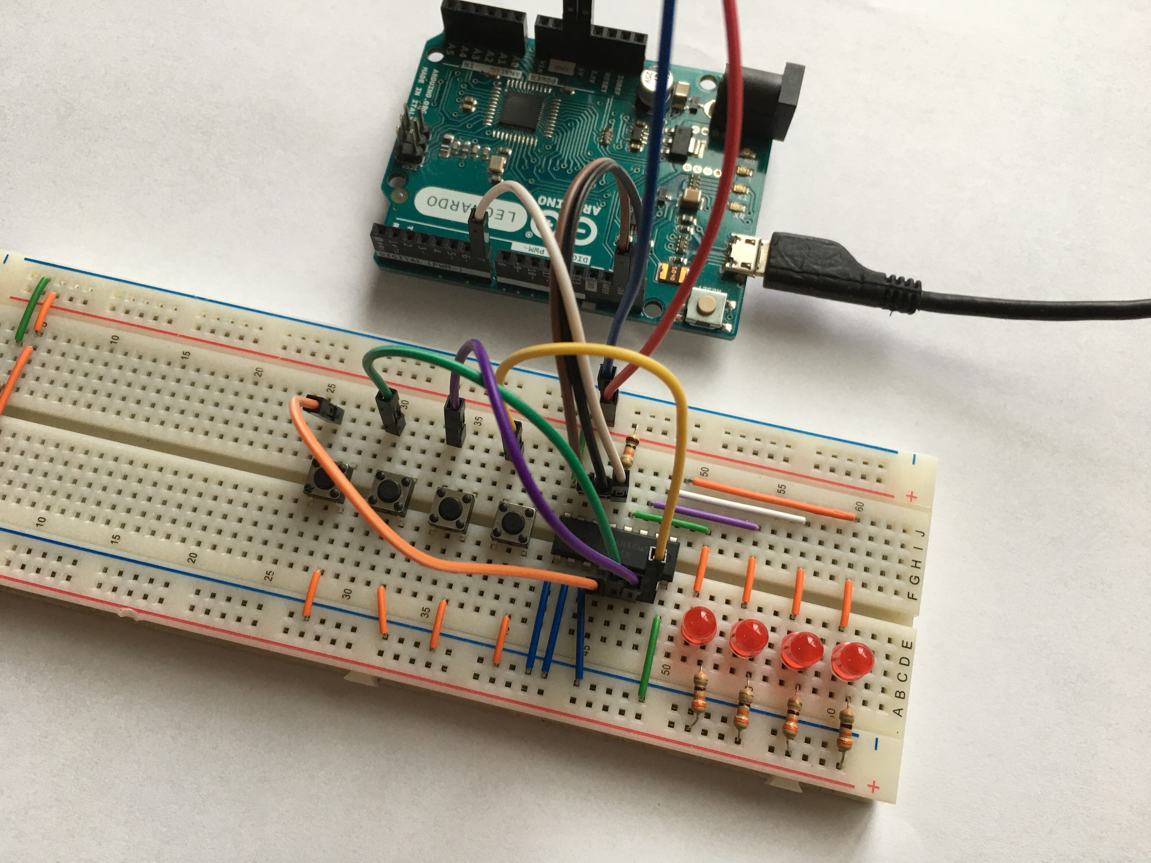
Consider the following simple system in which you can use four buttons to enter and accept code/password (defined as
CODE in source code). If correct, you will have an access to protected resources. System signals the fact of obtaining the appropriate authorizations by changing the status of the LEDs: the red one will go OFF and the green one will go ON for 2 seconds, after which the system will return to the default state, indicated by the red LED ON and the green one OFF.
|

|
| Colors of wires on schema are different to make clear which button is connected to which pin | |
The role of buttons is as follow (from left to the right):
- First, 0: allows to enter character (digit) 0.
- Second, 1: allows to enter character (digit) 1.
- Third, ENTER: allows to accept the entered sequence.
- Fourth, Delete: allows to delete the last entered character.
|
1 2 3 4 5 6 7 8 9 10 11 12 13 14 15 16 17 18 19 20 21 22 23 24 25 26 27 28 29 30 31 32 33 34 35 36 37 38 39 40 41 42 43 44 45 46 47 48 49 50 51 52 53 54 55 56 57 58 59 60 61 62 63 64 65 66 67 68 69 70 71 72 73 74 75 76 77 78 79 80 81 82 83 84 85 86 87 88 89 90 91 92 93 94 95 96 97 |
#define PIN_0 5 #define PIN_1 4 #define PIN_DELETE 3 #define PIN_ENTER 2 #define PIN_LED 7 #define MAX_CODE_LEN 32 #define CODE "10011" char codeArray[MAX_CODE_LEN+1]; byte codeLen = 0; void setup() { pinMode(PIN_0, INPUT); pinMode(PIN_1, INPUT); pinMode(PIN_DELETE, INPUT); pinMode(PIN_ENTER, INPUT); pinMode(PIN_LED, OUTPUT); Serial.begin(9600); digitalWrite(PIN_LED, LOW); for (int i=0; i<=MAX_CODE_LEN; i++){ codeArray[i] = '\0'; } Serial.println("Ready..."); } void loop() { if(digitalRead(PIN_0) == HIGH){ delay(20); while(digitalRead(PIN_0) == HIGH); delay(20); codeArray[codeLen] = '0'; codeArray[codeLen+1] = '\0'; codeLen += 1; if (codeLen == MAX_CODE_LEN) { codeLen -= 1; } Serial.println(codeArray); } else if(digitalRead(PIN_1) == HIGH){ delay(20); while(digitalRead(PIN_1) == HIGH); delay(20); codeArray[codeLen] = '1'; codeArray[codeLen+1] = '\0'; codeLen += 1; if (codeLen == MAX_CODE_LEN) { codeLen -= 1; } Serial.println(codeArray); } else if(digitalRead(PIN_DELETE) == HIGH){ delay(20); while(digitalRead(PIN_DELETE) == HIGH); delay(20); /* Funny bug if codeLen is declared as byte (to save memory for example). In such case codeLen -= 1 results in codeLen = 255 which is not lower than 0. codeLen -= 1; if (codeLen < 0) { codeLen = 0; } */ if (codeLen > 0) { codeLen -= 1; } codeArray[codeLen] = '\0'; Serial.println(codeArray); } else if(digitalRead(PIN_ENTER) == HIGH){ delay(20); while(digitalRead(PIN_ENTER) == HIGH); delay(20); if(strcmp(codeArray, CODE) == 0) { digitalWrite(PIN_LED, HIGH); Serial.println("Access granted..."); delay(2000); digitalWrite(PIN_LED, LOW); // Don't forget to clear whole buffer to prevent memory leaks. for (int i=0; i<=MAX_CODE_LEN; i++){ codeArray[i] = '\0'; } codeLen = 0; Serial.println("Ready..."); } Serial.println(codeArray); } } |
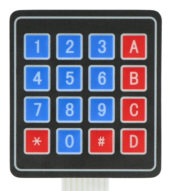
Both system and code is rather simple but I want to focus your attention on pins. At this moment you use 5 of total 19 pins of which 13 are digital and 6 are analog (but may be also used as digital). 14 pins are at your disposal, but will that be enough to handle typical alpha numeric characters? Typical, very simple membrane keyboard:
|
with only digits and some "function" keys require 8 pins. It is highly probable that you will lack of pins. This is how missing pins problem arise.
Recall voltage divider idea discussed in Voltage divider tutorial. General schema looks like it is showed on the following image

|
where the formula used to calculate $V_{out}$ takes a form
$$V_{out} = \frac{V_{in}R_{2}}{R_{1}+R_{2}}$$
|
$$V_{out} = \frac{V_{in}\cdot 0}{R_{1} + 0} = 0$$ | |
|
$$V_{out} = \frac{V_{in}R_{2}}{R_{1}+R_{2}} = \frac{V_{in}R_{2_{1}}}{R_{1}+R_{2_{1}}} = \frac{V_{in}}{\frac{R_{1}}{R_{2_{1}}}+1}$$ | |
|
$$V_{out} = \frac{V_{in}R_{2}}{R_{1}+R_{2}} = \frac{V_{in}(R_{2_{1}} + R_{2_{2}})}{R_{1}+R_{2_{1}}+R_{2_{2}}}= \frac{V_{in}}{\frac{R_{1}}{R_{2_{1}}+R_{2_{2}}}+1}$$ | |
|
$$V_{out} = \frac{V_{in}R_{2}}{R_{1}+R_{2}} = \frac{V_{in}(R_{2_{1}} + R_{2_{2}} + R_{2_{3}})}{R_{1}+R_{2_{1}}+R_{2_{2}}+R_{2_{3}}}= \frac{V_{in}}{\frac{R_{1}}{R_{2_{1}}+R_{2_{2}}+R_{2_{3}}}+1}$$ |


Examples given in previous subsection show few similar but different dividers. You can combine all of them into one schema:

|
How it works is explained in a set of images below.
|
|


When you press the first button, current bypass all resistors so you obtain voltage divider with only resistance $R_{1}$ without resistance $R_2$ ($R_2=0 Ohms$).
|
|


When you press the second button, current flows through only one resistor ($R_{2_{1}}$) so resistance $R_2$ is equal to $R_{2_{1}}$.
|
|


When you press the third button, current flows through two resistors ($R_{2_{2}}$ and $R_{2_{1}}$) so resistance $R_2$ is equal to sum of $R_{2_{2}}$ and $R_{2_{1}}$.
|
|


When you press the fourth button, current flows through three resistors ($R_{2_{3}}$, $R_{2_{2}}$ and $R_{2_{1}}$) so resistance $R_2$ is equal to sum of $R_{2_{3}}$, $R_{2_{2}}$ and $R_{2_{1}}$.
This way you have had created a variable voltage divider called a multiple voltage divider or more often a resistor ladder.
Now it's time to make a real test.
- Create circuit given in the schema below:

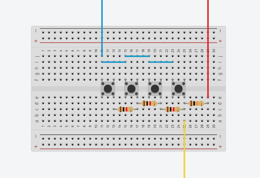
Left: Schema of resistor ladder. Right: Close to real view of resistor ladder
- Attach multimeter to our circuit:

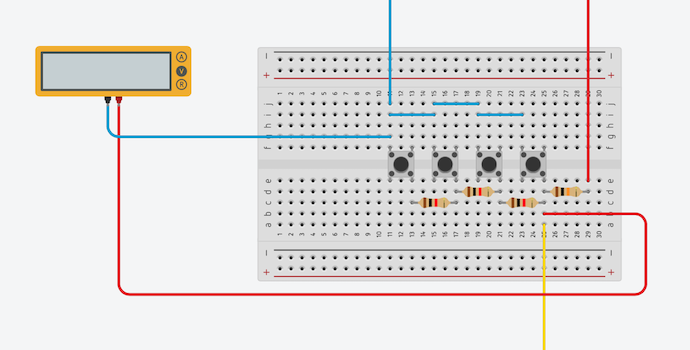
Left: Schema of ready to test resistor ladder circuit. Right: Close to real view of ready to test resistor ladder circuit - Use the following code to program Arduino
123456789101112131415161718192021222324#define VOLTAGE A0int sensorValue = 0;int i = 0;void printVolts(int val) {float voltage = val * (5.0 / 1023.0);Serial.print(" ADC value: ");Serial.print(val);Serial.print(", volts: ");Serial.println(voltage);}void setup() {Serial.begin(9600);}void loop() {sensorValue = analogRead(VOLTAGE);Serial.print(i);i++;printVolts(sensorValue);delay(1000);} -
Write down results: voltage displayed on multimeter and analog value read by Arduino and changed into numerical values by analog-digital converter (ADC in short). In this case I got:
Switch
pressedResistance value of variable
divider part $R_{2}$
(for constant $R_{1}=10kO$)Voltage used measured as integer
from ADCconverted to volts
from ADC valuemeasured by
multimetertheoretical
value1 0kO 0 0 0.0 0.00 0.0 2 $R_{2}$ = 1kO 0.98kO 95 0.46 0.47 0.45 3 $R_{2}+R_{2}$ = 1kO+1kO=2kO 1.97kO 180 0.89 0.83 0.83 4 $R_{2}+R_{2}+R_{2}$ = 1kO+1kO+1kO=3kO 2.95kO 238 1.16 1.16 1.15


This allows you to interpret each reading as a different button being pressed with a few lines of code -- see listing below. Obviously rather than telling the microcontroller to look for the exact values you expect the analog pin to read, you set a range of values that can be interpreted as belonging to a specific button. I do this by calculating the points halfway between each expected ADC reading (I called them midpoints) and set these as as the boundaries of my ranges (see also image):
| Switch | Range | ||
| from | to | midpoint | |
| 1 | 0 | 95 | 47 |
| 2 | 95 | 180 | 137 |
| 3 | 180 | 238 | 209 |
| 4 | 238 | 1023 | 630 |

|
| Divide 0-5 voltage range into intervals |
If you have all midpoints defining boundaries for each range, you can use them in software to detect which button you press:
|
1 2 3 4 5 6 7 8 9 10 11 12 13 14 15 16 17 18 19 20 21 22 23 24 25 |
#define VOLTAGE A0 int sensorValue = 0; int i = 0; int getButtonNumber(int val) { if (val <= 47) return 1; else if (val <= 137) return 2; else if (val <= 209) return 3; else if (val <= 630) return 4; else if (val <= 1023) return 0; } void setup() { Serial.begin(9600); } void loop() { sensorValue = analogRead(VOLTAGE); Serial.print(i); i++; Serial.print(" "); Serial.println(getButtonNumber(sensorValue)); delay(1000); } |
The downside is that output from voltage divider varies when different voltages are used so it require an update to your software.
So far, so good but this solution has two drawbacks which makes it working only for a project with a small number of buttons.
- Every time you change the number of buttons, you have to measure what have changed -- you have to measure ADC values for newly added button(s). Next you have to update your source code.
- What is worse, voltage resolution is not constant. The more buttons you have, the shortest voltage ranges you will have.
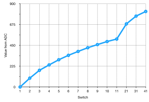
Adding another switches, each with a 1kO resistor, you obtain results presented in the table below. To make it more visible, also results for 21, 31 and 41 buttons obtained with 10kO resistors instead 10 times 1kO are included.Switch Range from to midpoint Midpoint
distance1 0 95 47 --- 2 95 180 137 90 3 180 238 209 66 4 238 294 266 57 5 294 342 318 52 6 342 384 363 45 7 384 424 404 41 8 424 458 441 37 9 458 491 474 33 10 491 518 504 30 11 518 21 682 31 766 41 816 1023 919
and depicted in the image:
The situation could be even worse if you use 1kO pull-up resistor:
Switch Range from to midpoint Midpoint
distance1 15 518 266 --- 2 518 687 602 336 3 687 769 728 126 4 769 820 794 66 5 820 853 836 42 6 853 877 865 29 7 877 895 886 21 8 895 909 902 16 9 909 920 914 12 10 920 930 925 11 11 930 21 974 31 990 41 998 1023 1010 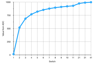
Variable and short voltage ranges may lead to errors both in code and in real devices as a result of noise and components tolerance. Anyway, magic numbers are always bad solution and should be avoided whenever possible. If you should somehow predict ADC value based on ADC resolution and number of buttons then you could implement better solution.


So, lets try find out resistors values to have equidistance measured in voltage, based on the following specification:
- $V_{in}=5V$,
- four buttons,
- pull-up resistor $R_{1}=1kO$,
- voltage distance $V_{d}=0.5$, e.g. $V_{S1}=0$ (voltage output for switch $S1$), $V_{S2}=V_{d}$ (voltage output for switch $S2$), $V_{S3}=2V_{d}$, $V_{S3}=3V_{d}$.
You know the input voltage, output voltage, and resistor $R_{1}$, but not $R_{2}$ which should be calculated. Starting from previously given formula:
$$V_{out} = \frac{V_{in}R_{2}}{R_{1}+R_{2}}$$
rearranging its components:
$$V_{out}(R_{1}+R_{2}) = V_{in}R_{2}$$
$$V_{out}R_{1}+V_{out}R_{2} = V_{in}R_{2}$$
$$V_{out}R_{1} = V_{in}R_{2}-V_{out}R_{2}$$
$$V_{out}R_{1} = R_{2}(V_{in}-V_{out})$$
you finally obtain formula for missing resistance $R_{2}$:
$$R_{2} = \frac{R_{1}V_{out}}{V_{in}-V_{out}}$$
Based on this formula and notation from the following schema you can calculate desired resistances $R_{21}$, $R_{22}$ and $R_{23}$.

|
- Calculations for $R_{21}$ -- in this case $V_{out}$ should be equal to 0.5V:
$$
R_{2} = R_{21} = \frac{R_{1}\cdot V_{out}}{V_{in}-V_{out}} = \frac{1.0 \cdot 0.5}{5.0 - 0.5} = \frac{0.5}{4.5} = 0.11
$$
To get resistance close to theoretical value of 0.11kO which is 110 Ohm, you will use one 100 Ohm resistor and one 10 Ohm so $R_{21}$ would be equal to 110 Ohm. - Calculations for $R_{22}$ -- in this case $V_{out}$ should be equal to 1.0V:
$$
R_{2} = R_{21} + R_{22}
$$
On the other hand you know that:
$$R_{2} = \frac{R_{1}V_{out}}{V_{in}-V_{out}}$$
so in consequence:
$$R_{21} + R_{22} = \frac{R_{1}V_{out}}{V_{in}-V_{out}}$$
and then:
$$R_{22} = \frac{R_{1}V_{out}}{V_{in}-V_{out}} - R_{21}$$
$$R_{22} = \frac{1.0 \cdot 1.0}{5.0-1.0} - 0.11 = \frac{1}{4} - 0.11 = 0.25 - 0.11 = 0.14$$
To get resistance close to theoretical value of 0.14kO which is 140 Ohm, you will use one 150 Ohm resistor so $R_{21}$ would be equal to 150 Ohm. - Calculations for $R_{23}$ -- in this case $V_{out}$ should be equal to 1.5V:
$$
R_{2} = R_{21} + R_{22} + R_{23}
$$
On the other hand you know that:
$$R_{2} = \frac{R_{1}V_{out}}{V_{in}-V_{out}}$$
so in consequence:
$$R_{21} + R_{22} + R_{23} = \frac{R_{1}V_{out}}{V_{in}-V_{out}}$$
and then:
$$R_{23} = \frac{R_{1}V_{out}}{V_{in}-V_{out}} - R_{21} - R_{22}$$
$$R_{23} = \frac{1.0 \cdot 1.5}{5.0-1.5} - 0.11 - 0.15 = \frac{1.5}{3.5} - 0.26 = 0.428 - 0.26 = 0.168$$
To get resistance close to theoretical value of 0.168kO which is 168 Ohm, you will use one 120 Ohm resistor and one 51 Ohm so $R_{23}$ would be equal to 171 Ohm.
The above procedure is quite mechanical and can be easily automated with simple code. Below you can find Python script implementing this procedure (even if you have no Python installed on your system, you can run it online, for example on OnlineGDB):
|
1 2 3 4 5 6 7 8 9 10 11 12 13 14 15 16 17 18 19 20 21 |
voltageInput = 5.0 numberOfButtons = 4 resistorPullUp = 1000 # In ohms voltageResolution = 0.5 resistanceToUse = { "3": 150 } voltageSum = 0.0 for button in range(1,numberOfButtons+1): voltageOutput = voltageResolution * (button-1) numerator = resistorPullUp * voltageOutput denominator = voltageInput - voltageOutput if str(button) in resistanceToUse and resistanceToUse[str(button)]: resistance = resistanceToUse[str(button)] else: resistance = round(numerator / denominator - voltageSum) voltageSum += resistance print(f"Button {button}: resistance {resistance} Ohms (vOut={voltageOutput})") |
The variable resistanceToUse defines resistances that must be used; for example you may require that third button should use 150 Ohms resistor:
|
1 2 3 |
resistanceToUse = { "3": 150 } |
When executed, above code should return the following output:
|
1 2 3 4 |
Button 1: resistance 0 Ohms (vOut=0.0) Button 2: resistance 111 Ohms (vOut=0.5) Button 3: resistance 150 Ohms (vOut=1.0) Button 4: resistance 168 Ohms (vOut=1.5) |
Finally you can implement more universal method for detecting the pin which was pressed:
|
1 2 3 4 5 6 7 8 9 10 11 12 13 14 15 16 17 18 19 20 21 22 23 24 25 26 27 28 |
#define VOLTAGE A0 #define VOLTAGE_RANGE 100 #define BUTTONS 4 int sensorValue = 0; int i = 0; int getButtonNumber(int val) { if (val > VOLTAGE_RANGE * BUTTONS - VOLTAGE_RANGE/2) { return 0; } else { return (val + VOLTAGE_RANGE/2)/VOLTAGE_RANGE + 1; } } void setup() { Serial.begin(9600); } void loop() { sensorValue = analogRead(VOLTAGE); Serial.print(i); i++; Serial.print(" "); Serial.println(getButtonNumber(sensorValue)); delay(1000); } |
and measure real voltage and ADC values as it is presented in the table below:
| Switch pressed |
Resistance value of variable divider part $R_{2}$ (for constant $R_{1}=1kO$) |
Resistance distance |
Voltage | |||||
| used | measured | calculated | used | as integer from ADC |
converted to volts from ADC value |
measured by multimeter |
theoretical value |
|
| 0 | --- | --- | --- | --- | 1023 | 5.00 | 4.95 | 5.00 |
| 1 | 0k$\Omega$ | 0 | 0 | 0 | 0 | 0.0 | 0.02 | 0.0 |
| 2 | $R_{21}$ = 110 $\Omega$ | 113 $\Omega$ | $R_{21}=110 \Omega$ | $R_{21}=110 \Omega$ | 100 | 0.5 | 0.51 | 0.5 |
| 3 | $R_{21}+R_{22}$ = 260 $\Omega$ | 260 $\Omega$ | $R_{22}=140 \Omega$ | $R_{22}=150 \Omega$ | 208 | 1.0 | 1.04 | 1.0 |
| 4 | $R_{21}+R_{22}+R_{23}$ = 431 $\Omega$ | 430 $\Omega$ | $R_{23}=168 \Omega$ | $R_{23}=171 \Omega$ | 306 | 1.5 | 1.51 | 1.5 |
Below you have a real life example of resistor ladder application:
You may ask: What if I press more than one button at once? For example: two or three? Nothing. Nothing in the sense that pressing multiple buttons at once is equivalent to pressing only one of them. Let's make a test in Tinkercad.
Start with pressing one button at a time (instead of buttons I use wire to make "hard" connection; this is due to inability to press more than one button in simulation which will be needed soon -- instead of pressing I make a connection):
No button is pressed:

|
First button is pressed:

|
Second button is pressed:

|
Third button is pressed:

|
Fourth button is pressed:

|
Now, press two buttons and more:
Fourth and third button is pressed:

|
In this case result is the same as you would press third button. If you continue this experiment you will not get different results in a sense that what you get agrees with corresponding one button case:
Fourth, third and second button is pressed:

|
All buttons are pressed:

|
Multiplexing is the generic term used to describe the operation of sending one or more analogue or digital signals over a common transmission line at different times or speeds. The device you use to do that is called a
multiplexer and demultiplexer. An electronic multiplexer (also mux or data selector) makes it possible for several signals to share one device or resource, for example, one A/D converter or one communication line, instead of having one device per input signal. It selects between several analog or digital input signals and forwards it to a single output line:
|
| Mechanical switch equivalent of 2-to-1 multiplexer |
You should be familiar with this concept, as every day you use it (or rather it is used by some devices) to transmit your data through an network:

|

|

|
| Data from multiple sources are transmitted through one communication chanel |
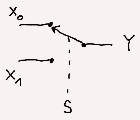
The selection of each input line in a multiplexer is controlled by an additional set of inputs called control lines and according to the binary condition of these control inputs, one selected data input is connected directly to the output. Normally, a multiplexer has an even number of $2^{n}$ input lines and a corresponding number of $n$ control inputs. An electronic multiplexer can be considered as a multiple-input, single-output switch. The schematic symbol for a multiplexer is an isosceles trapezoid with the longer parallel side containing the input pins and the short parallel side containing the output pin. The schematic below shows a 2-to-1 multiplexer (also denoted as 2:1 multiplexer or 2:1 mux) on the left and an equivalent switch on the right:

|

|
| Different symbols of 2-to-1 multiplexer | |
Multiplexers can be either digital circuits made from high speed logic gates used to switch digital or binary data or they can be analogue types using transistors, MOSFET’s or relays to switch one of the voltage or current inputs through to a single output.
To start out easy, you’ll create a multiplexer taking two inputs and a single selector line as it was depicted above. With inputs $X_{0}$ and $X_{1}$ and select line $S$, if $S$ is 0, the $X_{0}$ input will be the output $Y$. If S is 1, the $X_{1}$ will be the output $Y$.
To find a digital circuit implementing this functionality, you will apply approach described in my Logic gates tutorial. If you are not familiar with logic gates, it may be a good idea to read this material first.
You begin with creating corresponding truth table defining the dependence of the output signal on the value of the input signals:
| Inputs | Output | ||
|---|---|---|---|
| $S$ | $X_{0}$ | $X_{1}$ | $Y$ |
| 0 | 0 | 0 | 0 |
| 0 | 0 | 1 | 0 |
| 0 | 1 | 0 | 1 |
| 0 | 1 | 1 | 1 |
| 1 | 0 | 0 | 0 |
| 1 | 0 | 1 | 1 |
| 1 | 1 | 0 | 0 |
| 1 | 1 | 1 | 1 |
Having this table, you can derive a corresponding Boolean formula:
$$
\begin{align}
Y =
& \overline{S} \cdot X_0 \cdot \overline{X_1} + \overline{S} \cdot X_0 \cdot X_1 + S \cdot \overline{X_0} \cdot X_1 + S \cdot X_0 \cdot X_1 = \\
& \overline{S} \cdot X_0 \cdot (\overline{X_1} + X_1) + S \cdot X_1 \cdot (\overline{X_0} + X_0) = \\
& \overline{S} \cdot X_0 + S \cdot X_1\\
\end{align}
$$
The boolean formula for the 2-to-1 multiplexer looks like this:
$$Y= \overline{S} \cdot X_{0} + S \cdot X_{1}$$
or the same as programming logic expression:
|
1 |
Y = (~S && X0) || (S && X1) |
or in the pseudocode style:
|
1 |
Y = OR( AND(NOT(S), X0), AND(S, X1)) |
Based on the formulas given above, you can make a corresponding logic circuit:

|
Of course it can be completed also with other set of gates, for example NAND gates. From the previous material, Completeness of NAND gate set, you know that using only NAND gates you can have equivalents of all three basic gates: AND, OR and NOT as it is showed again below:

|
Using these "replacements" to the schema with basic set of gates you obtain:

|
This schema could be simplified. Let's introduce some additional symbols:

|
Now you can write:
$$
Y = \overline{E \cdot F} = \overline{\overline{C \cdot C} \cdot \overline{D \cdot D}}
$$
Because in Boolean algebra the following is true:
$$
X \cdot X = X
$$
you can write:
$$
Y = \overline{\overline{C} \cdot \overline{D}} = \overline{\overline{\overline{A \cdot A}} \cdot \overline{\overline{B \cdot B}}}
$$
Again from the law given above you obtain:
$$
Y = \overline{\overline{\overline{A}} \cdot \overline{\overline{B}}}
$$
and applying the following rule:
$$
\overline{\overline{X}} = X
$$
you finally get:
$$
Y = \overline{A \cdot B}
$$
Other words, none of the gate with output $C$, $D$, $E$ or $F$ is needed, and final schema of multiplexer build only with NAND gates looks like below:

|
You can combine two lower order multiplexers like 2:1 or 4:1 to get higher order multiplexer like 8:1. Now, for example you will implement a 4:1 multiplexer using a 2:1 multiplexer. To construct it, you have to combine three 2:1 multiplexer together, as I shown on the image below:

|
In result you have a circuit with:
- 4 input pins ($X_{0}$, $X_{1}$, $X_{2}$ and $X_{3}$),
- 2 control/select pins ($S_{0}$ and $S_{1}$)
- and one output pin ($Y$).
Dependence of the output signal on the combination of control signals $S_{0}$ and $S_{1}$ along with flow path of the signal is depicted below:

|
| Connecting input pin $X_{0}$ with output pin $Y$ by setting $(S_{0}, S_{1}) = (0,0)$ |

|
| Connecting input pin $X_{1}$ with output pin $Y$ by setting $(S_{0}, S_{1}) = (0,1)$ |

|
| Connecting input pin $X_{2}$ with output pin $Y$ by setting $(S_{0}, S_{1}) = (1,0)$ |

|
| Connecting input pin $X_{3}$ with output pin $Y$ by setting $(S_{0}, S_{1}) = (1,1)$ |
Conversely to multiplexer, a demultiplexer (or demux) takes only one input and pass through to one of multiple output lines, using a select line to choose which output the input goes to.

|

|
| Different symbols of 2-to-1 demultiplexer | |
To find a digital circuit implementing this functionality, first you have to create corresponding truth table:
| Inputs | Outputs | ||
|---|---|---|---|
| $S$ | $X$ | $Y_{0}$ | $Y_{1}$ |
| 0 | 0 | 0 | 0 |
| 0 | 1 | 1 | 0 |
| 1 | 0 | 0 | 0 |
| 1 | 1 | 0 | 1 |
Having this table, you can derive a corresponding Boolean formula which in case of the 1-to-2 demultiplexer is really simple and looks like this:
$$Y_{0}= \overline{S} \cdot X$$
$$Y_{1}= S \cdot X$$
or the same as programming logic expression:
|
1 2 |
Y0 = ~S && X Y1 = S && X |
or in the pseudocode style:
|
1 2 |
Y0 = AND(NOT(S), X) Y1 = AND(S, X) |
Based on the given above formulas, you can make a corresponding logic circuit:

|
Of course it can be completed also with other set of gates, for example only with NAND gates:

|
There are a lot of different ready to use (de)multiplexer.
- The basic trio of analog multiplexers stems from the venerable 4000-series CMOS logic chips: the 4051 is a single eight-way multiplexer, the 4052 has two four-way multiplexers, and the 4053 has three two-way switches.
- The 74HC405x series chips with higher switching speed or low-voltage analog multiplexers meant for battery-powered use: 74LV405x.
- The high-speed and low-resistance 3251, 3252, and 3253 series chips: CBT3251, FST3252, SN74CBT3253, etc.
In most cases multiplexer can work also as a demultiplexer, so further I will use the term multiplexer in both meanings.
In this part I will show how to work with
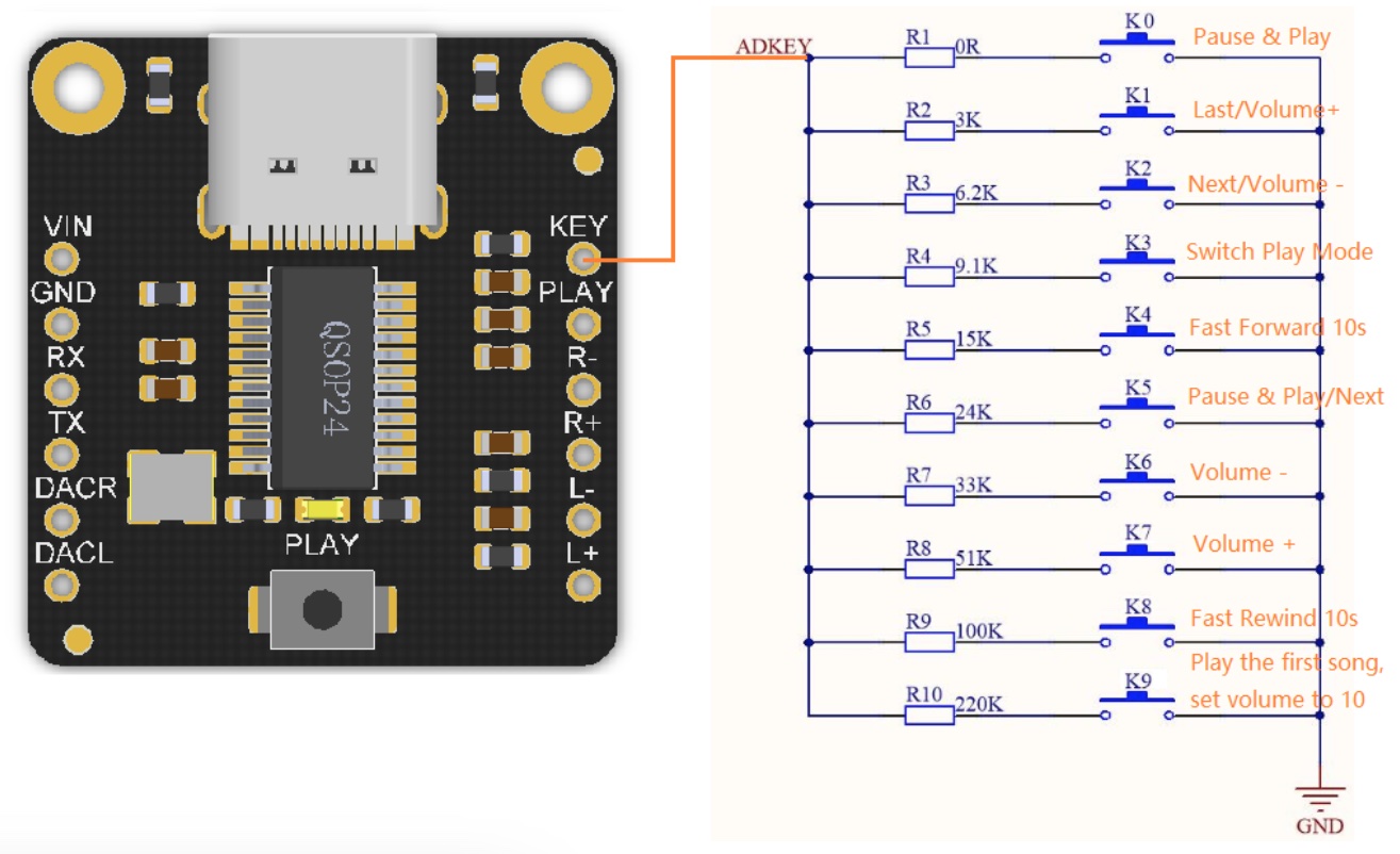
CD4051B and CD4052B chip (CD4051B, CD4052B, CD4053B data sheet CD4051 is an eight (8) channel multiplexer and has three control input named as A, B and C. These control inputs selects one of 8 channels to the output in order to obtain the desired connection. Channel I/O terminals became outputs and common O/I become input terminals when CD 4051 is used as a demultiplexer. Pinouts for all chips from this family are depicted on the image below and for CD4051 chip is summarized in the following table:
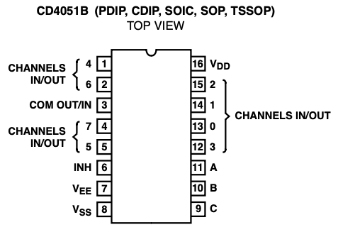
|

|

|
| Left: Pinouts of 4051 chip. Middle: Pinouts of 4052 chip. Right: Pinouts of 4053 chip. | ||
Pin |
Meaning | |
A |
selector line coding first bit of binary channel number | |
B |
selector line coding second bit of binary channel number | |
C |
selector line coding third bit of binary channel number | |
0-7 |
independent inputs/outputs channels | |
Vee |
negative supply voltage (connected to ground (GND) in our case) | |
Vss |
ground (GND, 0V) | |
Vdd |
positive supply voltage (from 5 to 20 volts) | |
COM AUT/IN |
common input/output | |
INH |
enable input active on LOW (connected to ground (GND) in our case) |
|

|
| Left: Basic schema to test CD4051 chip |
In this example you select which LED of set of four of them is turned on providing "address" on control lines connecting each manually either to HIGH (Vcc, +) or LOW (GND, -) which corresponds to binary values 1 and 0 respectively. For example, as it is shown on the image, to turn first LED on you have to provide control signal of value (A, B, C) = (0, 1, 0).
Static software channel selection
Let's improve above static hardware channel selection case and turn it into static software channel selection example. I show a very basic application accompanied by a very simple code. Connect all the components according to the schema given bellow:

|
| Left: Basic schema to test CD4051 chip |
and use the following code:
|
1 2 3 4 5 6 7 8 9 10 11 12 13 14 15 16 17 18 19 20 |
#define ZERO LOW #define ONE HIGH #define SELECT_PIN_A 2 #define SELECT_PIN_B 3 #define SELECT_PIN_C 4 void setup(){ pinMode(SELECT_PIN_A, INPUT); pinMode(SELECT_PIN_B, INPUT); pinMode(SELECT_PIN_C, INPUT); digitalWrite(SELECT_PIN_A, ZERO); digitalWrite(SELECT_PIN_B, ONE); digitalWrite(SELECT_PIN_C, ZERO); } void loop () { } |
Dynamic software channel selection
Mode: one input - multiple outputs
Of course the "address" doesn't have to be hardcoded and can change during code execution depending on the state of the system. To do this you need a piece of code to set address depending on the decimal number you provide. For example, binary equivalent of decimal number 3 is 011, so PIN_A of address should be set to HIGH, PIN_B should be set to HIGH and PIN_C should be set to LOW. To manipulate bits you can use standard binary operation (see function selectChannelV2 or selectChannelV3 below) as well as bitRead() function (see function selectChannelV1 below). You can write a lot of various code to accomplish this, below I present three of my implementations:
|
1 2 3 4 5 6 7 8 9 10 11 12 13 14 15 16 17 18 19 20 21 22 23 24 25 26 |
void selectChannelV1(byte number){ byte bitValue = bitRead(number, 0); digitalWrite(PIN_4051_SELECT_A, bitValue); bitValue = bitRead(number, 1); digitalWrite(PIN_4051_SELECT_B, bitValue); bitValue = bitRead(number, 2); digitalWrite(PIN_4051_SELECT_C, bitValue); } void selectChannelV2(byte number){ byte bitValue = (number & (1)) ? ONE : ZERO; digitalWrite(PIN_4051_SELECT_A, bitValue); bitValue = (number & (1<<1)) ? ONE : ZERO; digitalWrite(PIN_4051_SELECT_B, bitValue); bitValue = (number & (1<<2)) ? ONE : ZERO; digitalWrite(PIN_4051_SELECT_C, bitValue); } void selectChannelV3(byte number){ byte bitValue = (number & 1) ? ONE : ZERO; digitalWrite(PIN_4051_SELECT_A, bitValue); bitValue = (number & 2) ? ONE : ZERO; digitalWrite(PIN_4051_SELECT_B, bitValue); bitValue = (number & 4) ? ONE : ZERO; digitalWrite(PIN_4051_SELECT_C, bitValue); } |
If you change the "address" fast enough, you can keep all LEDs to appear as they would be in ON state. You can try the following code:
|
1 2 3 4 5 6 7 8 9 10 11 12 13 14 15 16 17 18 19 20 21 22 23 24 25 26 27 28 29 30 31 32 33 34 35 36 37 38 39 40 41 42 43 44 45 46 |
#define ZERO LOW #define ONE HIGH #define PIN_4051_SELECT_A 5 #define PIN_4051_SELECT_B 6 #define PIN_4051_SELECT_C 7 #define PIN_4051_IN_OUT 4 #define NUMBER_OF_4051_OUTPUT_CHANNELS 4 byte channelsOut[NUMBER_OF_4051_OUTPUT_CHANNELS] = {3, 0, 1, 2}; int channel; void selectChannelV3(byte number); void setup(){ pinMode(PIN_4051_SELECT_A, OUTPUT); pinMode(PIN_4051_SELECT_B, OUTPUT); pinMode(PIN_4051_SELECT_C, OUTPUT); pinMode(PIN_4051_IN_OUT, OUTPUT); digitalWrite(PIN_4051_SELECT_A, ONE); digitalWrite(PIN_4051_SELECT_B, ONE); digitalWrite(PIN_4051_SELECT_C, ONE); digitalWrite(PIN_4051_IN_OUT, HIGH); } void loop () { for (channel=0; channel<NUMBER_OF_4051_OUTPUT_CHANNELS; channel++) { selectChannelV3(channelsOut[channel]); delay(2); } } void selectChannelV3(byte number){ byte bitValue = (number & 1) ? ONE : ZERO; digitalWrite(PIN_4051_SELECT_A, bitValue); bitValue = (number & 2) ? ONE : ZERO; digitalWrite(PIN_4051_SELECT_B, bitValue); bitValue = (number & 4) ? ONE : ZERO; digitalWrite(PIN_4051_SELECT_C, bitValue); } |
The final result is dependent on your components. The following circuit worked for me:
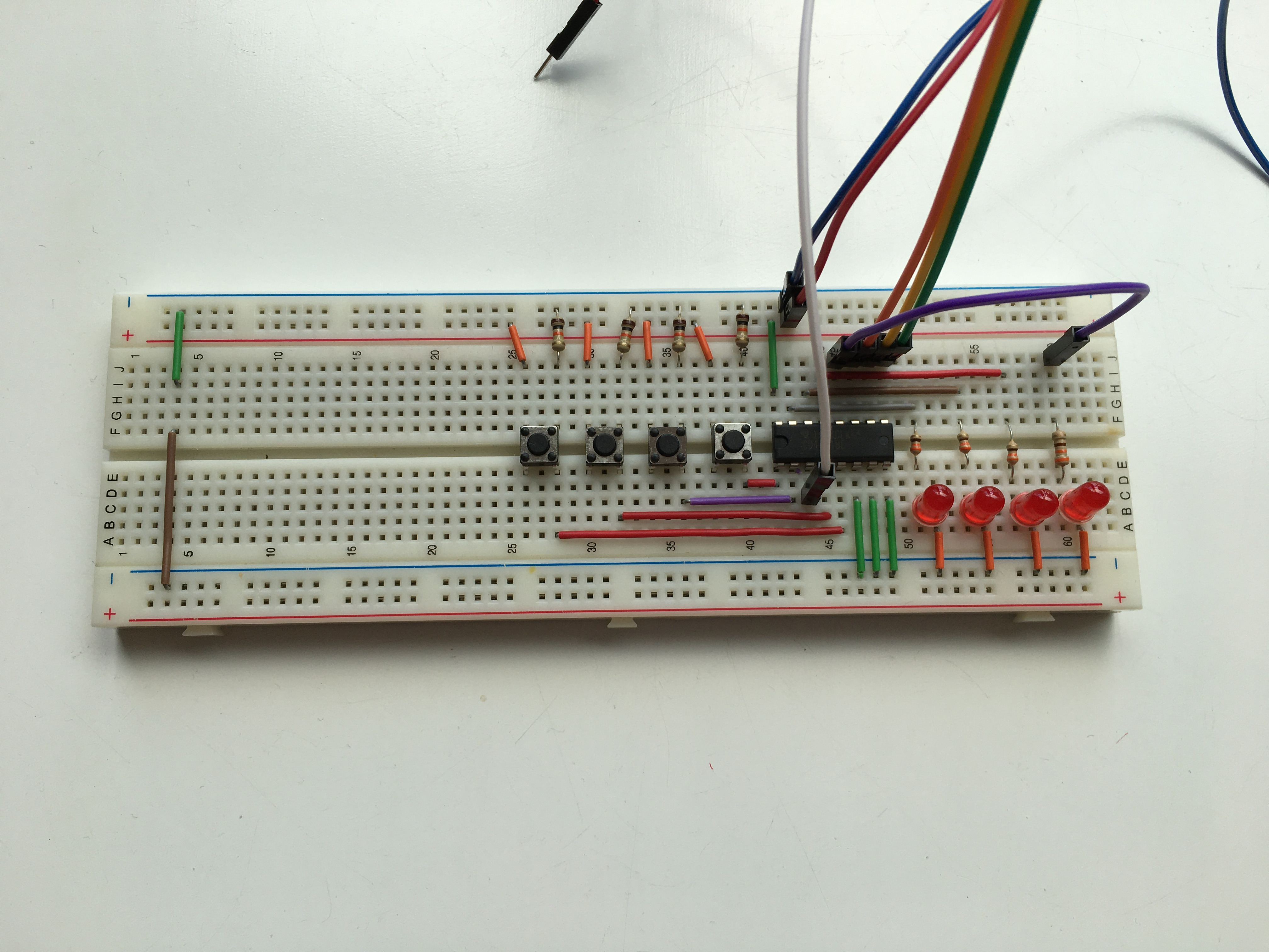
|
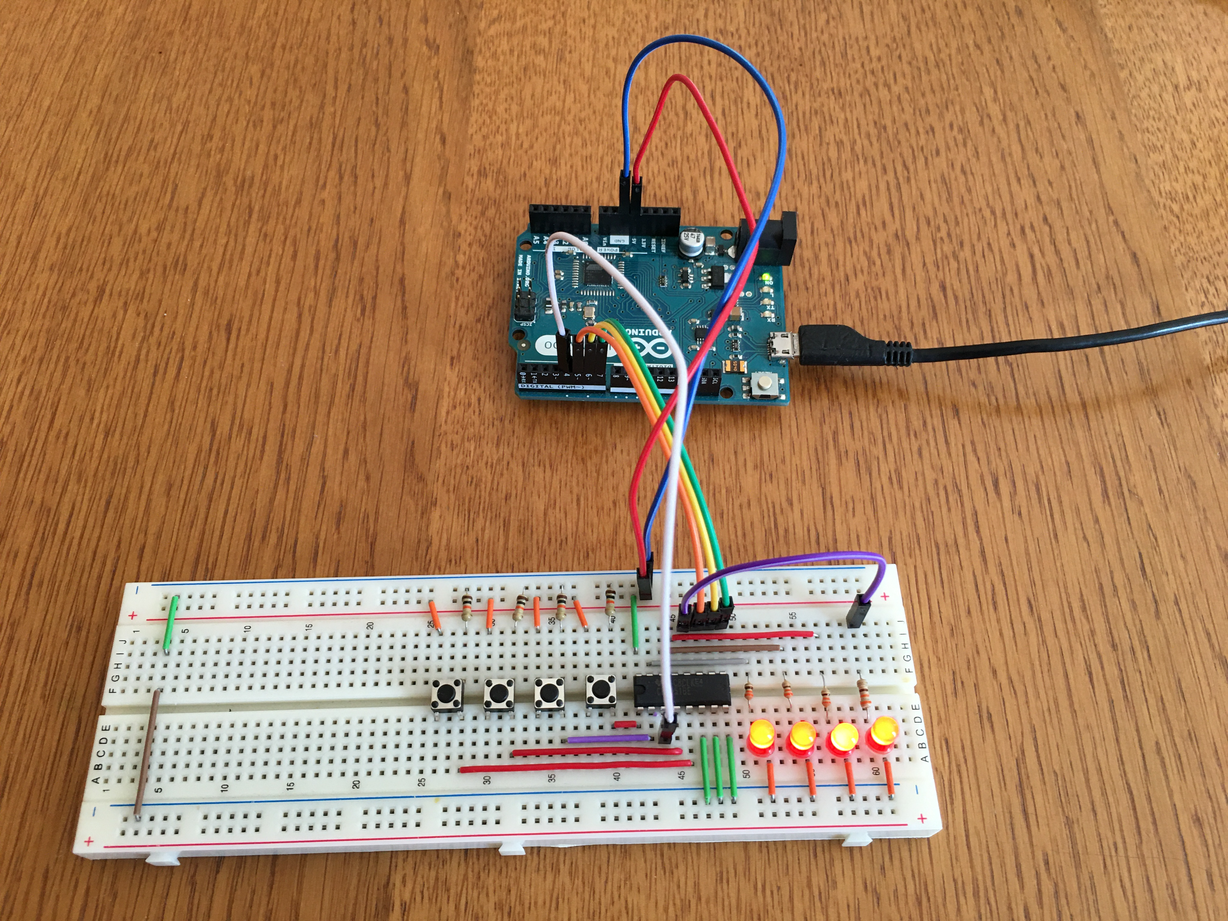
|
| Note: you don't need left part, with buttons, in this example, however you will use it in the next one | |
When you look at this circuit it seems that all LEDs are ON at the same time. This is only an impression caused by the imperfections of our senses. In fact, only one LED is powered at any given time; the others are OFF. This is much more visible when you look at the circuit, e.g. through the camera lens of your phone :
4051_example_03_work.movMode: multiple inputs - one output
Next example is closer to be a solution of an initial problem of being able to operate with many buttons. Instead of scan multiple output lines you will scan multiple inputs, each with one button attached to it.
Extend previous example and add to it four buttons:

|
|
| Note: you don't need right part, with LEDs, in this example | |
Our goal is to read state of many buttons (in example you will use 4 switches) using only one input. Try the following code:
|
1 2 3 4 5 6 7 8 9 10 11 12 13 14 15 16 17 18 19 20 21 22 23 24 25 26 27 28 29 30 31 32 33 34 35 36 37 38 39 40 41 42 43 44 45 46 47 48 49 50 51 52 53 54 55 56 57 58 59 60 61 62 63 64 65 66 67 68 69 |
#define FALSE 0 #define TRUE 1 #define ZERO LOW #define ONE HIGH #define PIN_4051_SELECT_A 5 #define PIN_4051_SELECT_B 6 #define PIN_4051_SELECT_C 7 #define PIN_4051_IN_OUT 4 #define NUMBER_OF_4051_INPUT_CHANNELS 4 byte channels[NUMBER_OF_4051_INPUT_CHANNELS] = {5, 7, 6, 4}; byte buttonStateChanged; byte channel; byte inputValue; byte switchState[NUMBER_OF_4051_INPUT_CHANNELS] = {LOW, LOW, LOW, LOW}; void selectChannelV3(byte number); void setup(){ Serial.begin(9600); pinMode(PIN_4051_SELECT_A, OUTPUT); pinMode(PIN_4051_SELECT_B, OUTPUT); pinMode(PIN_4051_SELECT_C, OUTPUT); pinMode(PIN_4051_IN_OUT, INPUT); digitalWrite(PIN_4051_SELECT_A, ONE); digitalWrite(PIN_4051_SELECT_B, ONE); digitalWrite(PIN_4051_SELECT_C, ONE); } void loop () { buttonStateChanged = FALSE; for(channel = 0; channel < NUMBER_OF_4051_INPUT_CHANNELS; channel++) { selectChannelV3(channels[channel]); inputValue = digitalRead(PIN_4051_IN_OUT); if (switchState[channel] != inputValue) { switchState[channel] = inputValue; buttonStateChanged = TRUE; } } if (buttonStateChanged == TRUE) { // Do some action depending on the buttons you press // Here you only print their states for(channel = 0; channel < NUMBER_OF_4051_INPUT_CHANNELS; channel++) { Serial.print(switchState[channel]==LOW? "- " : "H "); Serial.print(" "); } Serial.println(); } } void selectChannelV3(byte number){ byte bitValue = (number & 1) ? ONE : ZERO; digitalWrite(PIN_4051_SELECT_A, bitValue); bitValue = (number & 2) ? ONE : ZERO; digitalWrite(PIN_4051_SELECT_B, bitValue); bitValue = (number & 4) ? ONE : ZERO; digitalWrite(PIN_4051_SELECT_C, bitValue); } |
Below you have an example of my results with some comments:
|
1 2 3 4 5 6 7 8 9 10 11 12 |
13:38:52.767 -> H - - - <-- Press button 1 13:38:53.093 -> - - - - <-- Release button 1 13:38:53.830 -> - H - - <-- Press button 2 13:38:54.026 -> - - - - <-- Release button 2 13:38:54.688 -> - - H - <-- Press button 3 13:38:54.884 -> - - - - <-- Release button 3 13:38:55.509 -> - - - H <-- Press button 4 13:38:55.641 -> - - - - <-- Release button 4 13:38:57.976 -> H - - - <-- Press button 1 13:38:58.439 -> H - H - <-- Press button 3 while button 1 is pressed 13:39:00.659 -> - - H - <-- Release button 1 13:39:00.659 -> - - - - <-- Release button 3 |
Whatever you do with (de)multiplexer, always only one of many channels is physically connected with in/out pin. There is no chance to have for example multiple LEDs to be truly on -- you can only mimic this, as you have seen in a previous section. Multiplexers are pretty dumb. They just feeds signals through to the connected pins. Only the signal that is currently fed through can have anything to be done with it. So only one signal can have a value written on it or read from. There are no pullup resistors and interrupts.
Instead (de)multiplexer you can try expander. As it name stands, expander expanders something -- your pins. It gives you "extra" real in/out pins. You can read and write to all of the pins. Each one has facilities such as pull-up resistors, change notification interrupts, etc -- the kind of things you expect from real I/O pins.
If you ask, why I talk about multiplexers when you have expanders, the answer is as usual: because of money. Expanders are about four time more expensive than multiplexers:
Prices in Polish currency (on 2021-11-22):
|
1 2 3 4 5 6 7 |
Multiplexer: 4052 - 2PLN Expander: MCP23S08 - 10PLN PCF8574N - 7PLN PCF8574 - 8PLN |
Because expanders give you more options how you can use them, this section would be longer than previous. I will start from communication.
Multiplexer, at least the one I'm going to describe (PCF8574N), communicate with other components via the two-line bidirectional bus known as Inter-integrated Circuit, pronounced I-squared-C (I²C) or I2C. Actually you need 4 wires because you also use two power lines: the VCC and Ground.
The two data wires are:
- SDA - Serial Data (data line) and
- SCL - Serial Clock (clock line).
If you want to know more about the I2C technology please check out my Data transmission tutorial (not ready yet).
In this part I will show how to work with PCF8574 chip (NXP PCF8574 datasheet ![]() , Texas Instruments PCF8574 datasheet
, Texas Instruments PCF8574 datasheet ![]() )
)
Pinouts for typical PCF8574 chip enclosed in DIP16 package is depicted on the image below (you can also find this chip enclosed in SSOP20 package):
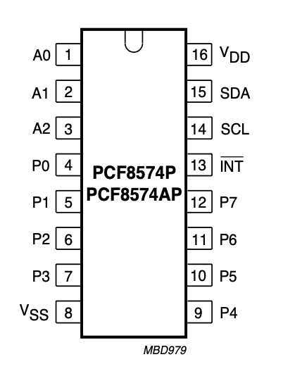
|

|

|
| Left: Pin configuration of PCF8574 chip in DIP16 package. Middle: Real photo of PCF8574. Right: Pin configuration of PCF8574 chip in SSOP20 package. | ||
Pin |
Meaning |
|---|---|
A0-A2 |
address input 0-2 |
P0-P7 |
quasi-bidirectional I/O 0-7 |
SCL |
serial clock line |
SDA |
serial data line |
VSS |
supply ground |
VDD |
supply voltage |
INT |
interrupt output (active LOW) |
As you can see, PCF8574 has three "address" pins: A0-A2. However they are not used in the way that multiplexer was. In this case address is not to select in/out pin but to define unique address of expander in I2C bus. Saying the truth, these pins are responsible only for part of real I2C address. Chips from the PCF8574 family have a 7-bit address. The first 3 bits of the address are given by the user by setting the pins A0, A1, A2. Another 4 are factory-set permanently. The PCF8574 chip has them set to 0100 and the PCF8574A chip set to 0111. In consequence you have the following options:
- for PCF8574:
- general address takes the form
0 1 0 0 A2 A1 A0, - the lowest address is
0 1 0 0 0 0 0which is 32 decimally and 0x20 hexadecimally, - the highest address is
0 1 0 0 1 1 1which is 39 decimally and 0x27 hexadecimally;
- general address takes the form
- for PCF8574A:
- general address takes the form
0 1 1 1 A2 A1 A0, - the lowest address is
0 1 1 1 0 0 0which is 56 decimally and 0x38 hexadecimally, - the highest address is
0 1 1 1 1 1 1which is 63 decimally and 0x3F hexadecimally.
- general address takes the form
The way you work with expander's pins is very similar to the way you work with microcontroller's pins. In this subsection I will present a set of examples executed on the following circuit:

|
|
There is no Arduino built-in library dedicated to PCF8574 -- instead you should install one on your own. There are a planty of them, all are similar but may differ slightly in details. To make my choice simpler, in the Arduino IDE Library Manager from dropdown Type I selected Recommended:
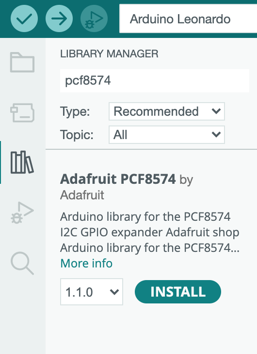
|
Then I installed the only library which was listed: the Adafruit PCF8574 by Adafruit library.
The PCF8574 is quite simple chip and when you use it you must obey some rule. The text cited below is taken from Adafruit PCF8574 I2C GPIO Expander / Overview
The PCF8574 is a common, and slightly unusual I2C expander for folks who are used to the MCP230xx series:
- First up, its very affordable - who doesn't love that?
- It has 8 I/O pins.
- Three I2C address select jumpers mean up to 8 expanders to one bus for 64 total GPIO added.
- Each pin can be an input with light pull-up or an output sink.
- IRQ output will automatically alert you when input pins change value.
- This chip does not have a pin direction register. You cannot set the pins to be input or output - instead each pin has two possible states. Basically you can think of it as an open-drain output with a 100K resistor pull-up built in.
- Option one: Lightly pulled up 'input' - by default it will read as a high logic level, but connecting the GPIO to ground will cause it to read as a low logic level.
- Option two: Strong 20mA low-driving transistor sink output. This means the output is 'forced' to be low and will always read as a low logic level.
The pin direction / state thing is a little odd but it actually works fine for many purposes as long as you know what to expect.
For example, if you want to read a button or switch, connect one side to the PCF and the other side to ground. Then set the pin to 'light pull-up input' When the button is pressed it will read low, when released it will read high.
If you want to control an LED, connect the anode to positive voltage through a resistor. When the PCF pin is set to 'light pull-up input' the LED will be off. When the PCF pin is set to 'strong ground output' the LED will connect to ground and turn on.
If you want to send a GPIO output logic level to some other device or peripheral, the light pull-up acts as high logic out, the strong ground output acts as low logic out.
If you want to receive a GPIO input logic level, set the pin to light pull-up and then read the pin to determine if the GPIO input is high or low.
Basically, the only thing to watch for is you cannot drive an LED that is expecting the expander GPIO to go high to turn on the LED, or connect a button input to a positive voltage without adding an additional pull-down resistor. If this is a bit confusing, worry not - all this stuff is taken care of for you in our Arduino PCF8574 library or CircuitPython/Python PCF8574 library - you can pretend it has input/output modes and the library will fake out what you are expecting.
With the following code you will implement very basic test scenario utilizing only LED part of the circuit -- you will blink only one (the right most) LED:
|
1 2 3 4 5 6 7 8 9 10 11 12 13 14 15 16 17 18 19 20 21 22 23 24 25 26 27 28 29 30 31 32 33 34 35 36 37 38 39 |
#include <Adafruit_PCF8574.h> #include <Wire.h> #define EXPANDER_ADDRESS 0x20 // 0x20 = 00100000_2 #define EX_PIN_LED_1 7 #define EX_PIN_LED_2 6 #define EX_PIN_LED_3 5 #define EX_PIN_LED_4 4 uint8_t exPinLed [] = { EX_PIN_LED_1, EX_PIN_LED_2, EX_PIN_LED_3, EX_PIN_LED_4 }; Adafruit_PCF8574 expander; uint8_t i; void setup() { if (!expander.begin(EXPANDER_ADDRESS, &Wire)) { while (10); } for (i=0; i<4; i++) { expander.pinMode(exPinLed[i], OUTPUT); expander.digitalWrite(exPinLed[i], HIGH); } } void loop() { expander.digitalWrite(EX_PIN_LED_4, LOW); delay(1000); expander.digitalWrite(EX_PIN_LED_4, HIGH); delay(1000); } |
In this example you will utilize a whole circuit, both LEDs and buttons. Pressing the button will turn ON a corresponding LED. Try the following code:
|
1 2 3 4 5 6 7 8 9 10 11 12 13 14 15 16 17 18 19 20 21 22 23 24 25 26 27 28 29 30 31 32 33 34 35 36 37 38 39 40 41 42 43 44 45 46 47 48 49 50 51 52 53 54 55 56 57 58 59 60 61 62 63 64 65 66 67 68 69 |
#include <Adafruit_PCF8574.h> #include <Wire.h> #define EXPANDER_ADDRESS 0x20 // 0x20 = 00100000_2 #define EX_PIN_LED_1 7 #define EX_PIN_LED_2 6 #define EX_PIN_LED_3 5 #define EX_PIN_LED_4 4 #define EX_PIN_BUTTON_1 0 #define EX_PIN_BUTTON_2 1 #define EX_PIN_BUTTON_3 2 #define EX_PIN_BUTTON_4 3 uint8_t exPinLed [] = { EX_PIN_LED_1, EX_PIN_LED_2, EX_PIN_LED_3, EX_PIN_LED_4 }; uint8_t exPinButton [] = { EX_PIN_BUTTON_1, EX_PIN_BUTTON_2, EX_PIN_BUTTON_3, EX_PIN_BUTTON_4 }; uint8_t ledState [] = { HIGH, HIGH, HIGH, HIGH }; Adafruit_PCF8574 expander; uint8_t i; void setup() { if (!expander.begin(EXPANDER_ADDRESS, &Wire)) { while (10); } for (i=0; i<4; i++) { expander.pinMode(exPinLed[i], OUTPUT); expander.pinMode(exPinButton[i], INPUT); expander.digitalWrite(exPinLed[i], HIGH); } } void loop() { for (i=0; i<4; i++) { if (expander.digitalRead(exPinButton[i]) == LOW) { if (ledState[i] != LOW) { expander.digitalWrite(exPinLed[i], LOW); ledState[i] = LOW; } } else { if (ledState[i] != HIGH) { expander.digitalWrite(exPinLed[i], HIGH); ledState[i] = HIGH; } } } delay(10); // A short debounce delay } |
Interrupt signal tells microcontroller that something is happen. With this, you don't have to constantly check the state of the pin on the chip -- you will be notified when a specific type of change occurs. You can read more about interrupts in my Interrupts section of a Multitasking tutorial.
|
1 2 3 4 5 6 7 8 9 10 11 12 13 14 15 16 17 18 19 20 21 22 23 24 25 26 27 28 29 30 31 32 33 34 35 36 37 38 39 40 41 42 43 44 45 46 47 48 49 50 51 52 53 54 55 56 57 58 59 60 61 62 63 64 65 66 67 68 69 70 71 72 73 74 75 76 77 78 79 80 81 82 83 84 85 86 87 88 89 90 91 92 93 94 95 96 |
#include <Adafruit_PCF8574.h> #include <Wire.h> #define EXPANDER_ADDRESS 0x20 // 0x20 = 00100000_2 #define MICROCONTROLLER_PIN_IRQ 7 // Make sure this pin is possible to make IRQ input #define EX_PIN_LED_1 7 #define EX_PIN_LED_2 6 #define EX_PIN_LED_3 5 #define EX_PIN_LED_4 4 #define EX_PIN_BUTTON_1 0 #define EX_PIN_BUTTON_2 1 #define EX_PIN_BUTTON_3 2 #define EX_PIN_BUTTON_4 3 uint8_t exPinLed [] = { EX_PIN_LED_1, EX_PIN_LED_2, EX_PIN_LED_3, EX_PIN_LED_4 }; uint8_t exPinButton [] = { EX_PIN_BUTTON_1, EX_PIN_BUTTON_2, EX_PIN_BUTTON_3, EX_PIN_BUTTON_4 }; uint8_t ledState [] = { LOW, LOW, LOW, LOW }; Adafruit_PCF8574 expander; uint8_t i; // A flag to make sure I don't enter the interrupt more than once volatile bool inIRQ = false; void setup() { if (!expander.begin(EXPANDER_ADDRESS, &Wire)) { while (10); } for (i=0; i<4; i++) { expander.pinMode(exPinLed[i], OUTPUT); expander.pinMode(exPinButton[i], INPUT); expander.digitalWrite(exPinLed[i], HIGH); } pinMode(MICROCONTROLLER_PIN_IRQ, INPUT); attachInterrupt( digitalPinToInterrupt(MICROCONTROLLER_PIN_IRQ), isrButtonPressed, CHANGE ); } void isrButtonPressed(void) { if (inIRQ) { return; // I am already handling an irq so return to not collide } inIRQ = true; interrupts(); // Arduino UNO seems to require that we turn on interrupts for I2C to work for (i=0; i<4; i++) { if (expander.digitalRead(exPinButton[i]) == LOW) { if (ledState[i] != LOW) { expander.digitalWrite(exPinLed[i], LOW); ledState[i] = LOW; } } else { if (ledState[i] != HIGH) { expander.digitalWrite(exPinLed[i], HIGH); ledState[i] = HIGH; } } } inIRQ = false; } void loop() { digitalWrite(LED_BUILTIN, HIGH); delay(500); digitalWrite(LED_BUILTIN, LOW); delay(1000); } |