
- A little bit of theory
- A little bit of application
- A little bit of practice
- Step 1: What do we want our logic circuit will do?
- Step 2: Define input-output relationship
- Step 3: Find Boolean expressions equivalent to our truth table
- Step 4: Simplify Boolean expressions
- Step 5: Prepare logic circuit based on Bolean expressions
- Step 6: Use real chips to implement logic circuit we have found
- Exercise 1
- Exercise 2
The word algebra has several related meanings in mathematics, but we will focus only on one of them. We will use a word algebra to denote a set of elements related with a set of operations over this set's elements.
Let's define a six-tuple $T=(B, AND, OR, NOT, 0, 1)$ consisting of a
- set $B$,
- two binary operations over elements from set $B$ called AND ($\cdot$) and OR (+),
- one unary operation called NOT (line over symbol, like $\overline{x}$) and,
- two distinct elements 0 and 1; both from set $B$.
Sometimes instead of AND we use $\cdot$, instead of OR we use $+$ and instead of NOT we use a line over a symbol like $\overline{x}$.
Next, for all elements $a$, $b$ and $c$ of $B$, define a set $A$ of the following axioms
\begin{align*}
a + (b + c) &= (a + b) + c & a \cdot (b \cdot c) &= (a \cdot b) \cdot c & \text{associativity}\\
a + b &= b + a & a \cdot b &= b \cdot a & \text{commutativity}\\
a + 0 &= a & a \cdot 1 &= a & \text{identity}\\
a + (b \cdot c) &= (a + b) \cdot (a + c) & a \cdot (b + c) &= (a \cdot b) + (a \cdot c) & \text{distributivity}\\
a + \overline{a} &= 1 & a \cdot \overline{a} &= 0 & \text{complements}
\end{align*}
Notice that above axioms shows some duality: every time we replace $+$ by $\cdot$ and 0 by 1 or reverse, we obtain second form. For example from $a + 0 = a$ we obtain $a \cdot 1 = a$. Boolean algebra is a six-tuple $T$ such that all the axioms from set $A$ hold.
With the axioms we can proof many different things and formulas. All of them are important, but one is very often used: De Morgan's laws
\begin{align*}
\overline{a + b} &= \overline{a}\cdot \overline{b}\\
\overline{a \cdot b} &= \overline{a} + \overline{b}
\end{align*}
From our point of view the most important is the simplest Boolean algebra, the two-element Boolean algebra, which has only two elements, 0 and 1.
From the axioms we can derive a set of rules for operations AND, OR and NOT
NOT 1 = 0
Proof:
a OR 0 = a
a OR NOT a = 1substituting a := 1 we obtain
1 OR 0 = 1
1 OR NOT 1 = 1and in consequence
NOT 1 = 0
NOT 0 = 1
Proof: By analogy we can proof NOT 0 = 1================================================================================
0 AND 0 = 0
Proof:
0 AND 0 = [from identity] = (0 AND 0) OR 0 =
= [from complements] = (0 AND 0) OR (0 AND (NOT 0)) =
= [from NOT 0 = 1] = (0 AND 0) OR (0 AND 1) =
= [from distributivity] = 0 AND (0 OR 1) =
= [from comutativity] = 0 AND (1 OR 0) =
= [from identity] = 0 AND 1 =
= [from NOT 0 = 1] = 0 AND (NOT 0) =
= [from complements] = 00 AND 1 = 0
Proof: from identity a AND 1 = a1 AND 0 = 0
Proof: from comutativity a AND b = b AND a and next we have previous case1 AND 1 = 1
Proof: from identity a AND 1 = a================================================================================
0 OR 0 = 0
Proof: from a OR 0 = a0 OR 1 = 1
Proof: from comutativity a OR b = b OR a and next we have next case1 OR 0 = 1
Proof: from a OR 0 = a1 OR 1 = 1
Proof:
By analogy to 0 AND 0 = 0
In most cases we draw the above set of rules in the form of truth table
| a | b | AND(a, b) | OR(a, b) | NOT(a) |
|---|---|---|---|---|
| 0 | 0 | 0 | 0 | 1 |
| 0 | 1 | 0 | 1 | 1 |
| 1 | 0 | 0 | 1 | 0 |
| 1 | 1 | 1 | 1 | 0 |
Boolean algebra has applications in logic, interpreting 0 as FALSE, 1 as TRUE. The two-element Boolean algebra is also used for circuit design in electrical engineering; here 0 and 1 represent the two different states of one bit in a digital circuit, typically HIGH and LOW voltage. Circuits are described by expressions containing variables, and two such expressions are equal for all values of the variables if and only if the corresponding circuits have the same input-output behavior. Furthermore, every possible input-output behavior can be modeled by a suitable Boolean expression. This makes Bolean algebra a perfect tool we can use during logic circuit design.
What is interesting, Bool introduced his algebra in a book The Mathematical Analysis of Logic (1847), and set forth more fully in his An Investigation of the Laws of Thought (1854). What could be realy depressing for any of us who wants to be a famous scientist is a fact that, during his lifetime, his work seemed to have no practical applications at all. It took a few decades to find application for this algebra. In 1930s Claude Shannon encountered it while studying at MIT, and in 1938 he published a paper describing how Boolean analysis could be applied to circuits using relays. This had immediate practical applications, as telephone networks were growing rapidly, creating complicated switching problems.
First note that we can define four different unary operators
a o1(a) o2(a) o3(a) o4(a)

0 1     0     1     0

1 1     1     0     0

o1 - verum (afirmative operator; tautology)

o2 - assertion (projection)

o3 - operator NOT (negation)

o4 - falsum
and sixteen different binary operators
a b  o1  o2  o3  o4  o5  o6  o7  o8  o9 o10 o11 o12 o13 o14 o15 o16

0 0  0   1   0   1   0   1   0   1   0   1   0   1   0   1   0   1

0 1  0   0   1   1   0   0   1   1   0   0   1   1   0   0   1   1

1 0  0   0   0   0   1   1   1   1   0   0   0   0   1   1   1   1

1 1  0   0   0   0   0   0   0   0   1   1   1   1   1   1   1   1

 o1 - contradiction

 o2 - NOR = NOT OR

 o3 - converse nonimplication

 o4 - negation

 o5 - material nonimplication

 o6 - negation

 o7 - XOR (exclusive disjunction)

 o8 - NAND = NOT AND

 o9 - AND

o10 - XNOR

o11 - projection function

o12 - material implication (rule of interference)

o13 - projection function

o14 - converse implication

o15 - OR

o16 - tautology
Generally, in computer science, among all of logic functions we use six of them
AND, OR, NOT, NAND, NOR, XOR
These logic functions were defined by logic operators in previous section: AND as o9, OR as o15, NOT as o3, NAND as o8, NOR as o2, XOR as 07.
In electronics, these logic functions are implemented as logic gate wich are a physical devices implementing a Boolean function. The following set of symbols is used to denote appropriate logic gate (realising appropriate logic function)
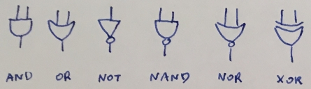
Having a given logic circuit (a set of connected logic gates) we can say, how this set will react in response to input signals. Other words, based on logic gates connections schema we can create input-output relationship table (truth table for this circuit).
The question is if all of them are unique in a sense that are not replaceable by combination of two or more other operators.
In logic, a functionally complete set of logical connectives or Boolean operators is one which can be used to express all possible truth tables by combining members of the set into a Boolean expression. A well-known complete set of connectives is { AND, NOT } and OR, NOT. What can be surprising, the singleton sets NAND and NOR are also functionally complete. Other words, there is a combination of only NAND (or only NOR) gates such that behaves like AND gate, other combination to get OR gate behavior and third combination to get NOT gate functionality.
From the point of view of digital electronics, functional completeness means that every possible logic gate can be realized as a network of gates of the types prescribed by the set. In particular, all logic gates can be assembled from either only binary NAND gates, or only binary NOR gates.
We will show how to get AND, OR and NOT logic circuit based on NAND gates.
Todo (id=no todo id): logic_gates:improve images quality
- NOT
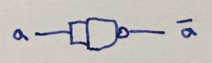
$$
NAND(a, a) = NOT(AND(a, a)) = NOT(a)
$$
or the same in other form
$$
\overline{a \cdot a} = \overline{a}.
$$ - AND
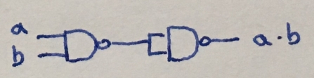
\begin{align*}
NAND(NAND(a, b), NAND(a, b)) &= NOT(AND(NAND(a, b), NAND(a, b))) = NOT(NAND(a,b))\\
&= NOT(NOT(AND(a,b)))
\end{align*}
or the same in other form
$$
\overline{\overline{a \cdot b} \cdot \overline{a \cdot b}} = \overline{\overline{a \cdot b}} = a \cdot b.
$$ - OR
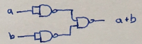
\begin{align*}
NAND(NAND(a, a), NAND(b, b)) &= NOT(AND(NOT(a), NOT(b))) = OR(NOT(NOT(a)), NOT(NOT(b)))\\
&= OR(a, b)
\end{align*}
or the same in other form
$$
\overline{\overline{a \cdot a} \cdot \overline{b \cdot b}} = \overline{\overline{a} \cdot \overline{b}} = \overline{\overline{a}} + \overline{\overline{b}} = a + b.
$$
We will show how to get AND logic circuit based on OR and NOT gates.
$$
NOT(OR(NOT(a), NOT(b))) = AND(NOT(NOT(a)), NOT(NOT(b))) = AND(a, b)
$$
or the same in other form
$$
\overline{\overline{a}+\overline{b}} = \overline{\overline{a}} \cdot \overline{\overline{b}} = a \cdot b.
$$
As an example consider very useful combinational logic circuit known as digital comparator circuit. The purpose of a digital comparator is to compare two numbers: $x$ and $y$, and produce an output condition or flag depending upon the result of the comparison. For example, a magnitude comparator of two 1-bits inputs would produce the following three output conditions $x \gt y$, $x=y$, $x \lt y$ depending on whether $x$ is greater than $y$, $x$ is equal to $y$, and $x$ is less than $y$
There are two main types of digital comparator available and these are.
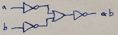
- Identity comparator - an identity comparator is a digital comparator that has only one output terminal for when $x = y$.
- Magnitude comparator - a magnitude comparator is a digital comparator which has three output terminals, one each for equality ($x = y$), greater than ($x > y$) and less than ($x < y$).
Truth table and logic circuit for this comparator is presented below
| Inputs | Output | |
|---|---|---|
| x | y | x = y |
| 0 | 0 | 1 |
| 0 | 1 | 0 |
| 1 | 0 | 0 |
| 1 | 1 | 1 |

How to verify correctness of these circuits I will show explaining magnitude comparator below.
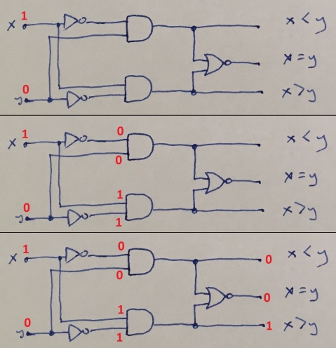
Truth table and logic circuit for this comparator is presented below
| Inputs | Outputs | |||
|---|---|---|---|---|
| x | y | x = y | x > y | x < y |
| 0 | 0 | 1 | 0 | 0 |
| 0 | 1 | 0 | 0 | 1 |
| 1 | 0 | 0 | 1 | 0 |
| 1 | 1 | 1 | 0 | 0 |
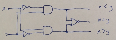
To verify that given logic circuit works correctly we can draw a signal flow as I did below
Please check Exercise 1 where you will find close to real magnitude comparator circuit I made in Tinkercad.
Now let's reverse the problem from the previous section: How to find a logic circuit realising predefined input-output relationship? We will show one method without diving to much into details.
Todo (id=no todo id): logic_gates:write a pages about logic circuit design, Carnaugh maps etc.
The aim of the logic circuit we want to create is to adding two 1-bit numbers. Yes, it is very simple task, but 1-bit adder is a component of more complicated 8-bit, 16-bit, and generaly n-bit adders.
I assume that you have basic knowledge about place-value notation, especially base-2 system and you know that binary number 10 is equal to decimal 2 (we will write this as $10_{2}=2_{10}$). As for every place-value system, it is enough to focus on one position, because other positions are calculated with the same manner, taking into account carry signals. We have the following variants adding two 1-bit numbers
x=0 x=0 x=1 x=1
y=0 y=1 y=0 y=1+--------- carry signal (carry out)
|
1
0 0 1 1 -- x
0 + 1 + 0 + 1 + -- y
----- ----- ----- -----
0 1 1 10
Base on these variants we can create truth table for 1-bit adder
| Inputs | Outputs | ||
|---|---|---|---|
| x | y | Value ($v$) | Carry out ($c_{out}$) |
| 0 | 0 | 0 | 0 |
| 0 | 1 | 1 | 0 |
| 1 | 0 | 1 | 0 |
| 1 | 1 | 0 | 1 |
Now we will incorporate into above carry signal from previous position
carry_in=0
x=0 x=0 x=1 x=1
y=0 y=1 y=0 y=10 0 0 0 -- carry in
0 0 1 1 -- x
0 + 1 + 0 + 1 + -- y
----- ----- ----- -----
0 1 1 10carry_in=1
x=0 x=0 x=1 x=1
y=0 y=1 y=0 y=11 1 1 1 -- carry in
0 0 1 1 -- x
0 + 1 + 0 + 1 + -- y
----- ----- ----- -----
1 10 10 11
Base on these variants we can create truth table for 1-bit adder
| Inputs | Outputs | |||
|---|---|---|---|---|
| Carry in ($c_{in}$) | x | y | Value ($v$) | Carry out ($c_{out}$) |
| 0 | 0 | 0 | 0 | 0 |
| 0 | 0 | 1 | 1 | 0 |
| 0 | 1 | 0 | 1 | 0 |
| 0 | 1 | 1 | 0 | 1 |
| 1 | 0 | 0 | 1 | 0 |
| 1 | 0 | 1 | 0 | 1 |
| 1 | 1 | 0 | 0 | 1 |
| 1 | 1 | 1 | 1 | 1 |
Let's start from carru out signal, as it is easier one. To create an expression we have to find all cases when carry out is 1 (TRUE) - there are four such cases:
- carry out is 1 when carry in is 0, x=1, y=1,
- or when carry in is 1, x=0, y=1,
- or when carry in is 1, x=1, y=0,
- or finally when carry in is 1, x=1, y=1.
Other words we can write that as
c_out = 1 if and only if (

  (c_in, x, y) = (0, 1, 1) or

  (c_in, x, y) = (1, 0, 1) or

  (c_in, x, y) = (1, 1, 0) or

  (c_in, x, y) = (1, 1, 1)

)
or equivalently
c_out = 1 if and only if (

  (NOT(c_in), x, y) = (1, 1, 1) or

  (c_in, NOT(x), y) = (1, 1, 1) or

  (c_in, x, NOT(y)) = (1, 1, 1) or

  (c_in, x, y) = (1, 1, 1)

)
and finally in more compact form
$$
c_{out} = \overline{c_{in}}xy + c_{in}\overline{x}y + c_{in}x\overline{y} + c_{in}xy.
$$
We can verify this formula taking all 0-1 three-tuples and compare results with truth table given above. We will check it for two of them
- For three-tuple $(c_{in}, x, y) = (0, 1, 1)$ we obtain
$$
c_{out} = \overline{c_{in}}xy + c_{in}\overline{x}y + c_{in}x\overline{y} + c_{in}xy = \overline{0}11 + 0\overline{1}1 + 01\overline{1} + 011 = 111 + 001 + 010 + 011 = 1 + 0 + 0 + 0 = 1.
$$ - For three-tuple $(c_{in}, x, y) = (1, 0, 0)$ we obtain
$$
c_{out} = \overline{c_{in}}xy + c_{in}\overline{x}y + c_{in}x\overline{y} + c_{in}xy = \overline{1}00 + 1\overline{0}0 + 10\overline{0} + 100 = 000 + 110 + 101 + 100 = 0 + 0 + 0 + 0 = 0.
$$
Using the same tehnique as for carry out signal, we obtain
$$
v = \overline{c_{in}}\overline{x}y + \overline{c_{in}}x\overline{y} + c_{in}\overline{x}\overline{y} + c_{in}xy.
$$
According to Boolean algebra's rules we can simplify formulas from previous section as follow.
Formula for $c_{out}$:
\begin{align*}
c_{out} & = \overline{c_{in}}xy + c_{in}\overline{x}y + c_{in}x\overline{y} + c_{in}xy\\
& \overset{(1)}{=} \overline{c_{in}}xy + c_{in}\overline{x}y + c_{in}x\overline{y} + c_{in}xy + c_{in}xy + c_{in}xy\\
& \overset{(2)}{=} \overline{c_{in}}xy + c_{in}xy + c_{in}\overline{x}y + c_{in}xy + c_{in}x\overline{y} + c_{in}xy\\
& \overset{(3)}{=} (\overline{c_{in}}xy + c_{in}xy) + (c_{in}\overline{x}y + c_{in}xy) + (c_{in}x\overline{y} + c_{in}xy)\\
& \overset{(4)}{=} xy(\overline{c_{in}} + c_{in}) + c_{in}y(\overline{x} + x) + c_{in}x(\overline{y} + y)\\
& \overset{(5)}{=} xy(1) + c_{in}y(1) + c_{in}x(1)\\
& \overset{(6)}{=} xy + c_{in}y + c_{in}x.
\end{align*}
where
- For every Boolean expression, we can take one of its term and repeat it as many times as we want, for example
\begin{align*}
a & = a + a + a + a\\
a \cdot b & = a \cdot a \cdot a \cdot b \cdot b
\end{align*}
In this case we did it with a term $c_{in}xy$. - Simply rearange terms.
- Grup terms with brackets.
- Use distributivity to extract common term.
- Compute values in brackets.
- Use identity.
Formula for $v$:
\begin{align*}
v & = \overline{c_{in}}\overline{x}y + \overline{c_{in}}x\overline{y} + c_{in}\overline{x}\overline{y} + c_{in}xy\\
& \overset{(1)}{=} \overline{c_{in}}(\overline{x}y + x\overline{y}) + c_{in}(\overline{x}\overline{y} + xy)
\end{align*}
where
- Use distributivity to extract common term.
Now it is important to notice that introducing new symbols $a$ and $b$ such that
\begin{align*}
a &= \overline{x}y + x\overline{y}\\
b &= \overline{x}\overline{y} + xy
\end{align*}
we obtain that
$$
\overline{a} = b
$$
Proof of this is not difficult (we will use De Morgan's laws: $\overline{x + y} = \overline{x}\cdot \overline{y}$ and $\overline{x \cdot y} = \overline{x} + \overline{y}$)
$$
\overline{\overline{x}y + x\overline{y}} = \overline{(\overline{x}y)} \cdot \overline{(x\overline{y})} = (\overline{x} + y) \cdot (x + \overline{y}) = (x+\overline{y})x + (x+\overline{y})y = \overline{x}\overline{y}+xy.
$$
Finally we get
$$
v = \overline{c_{in}}a + c_{in}\overline{a}.
$$
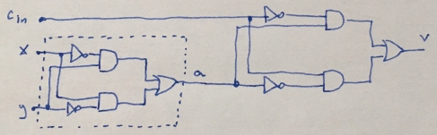
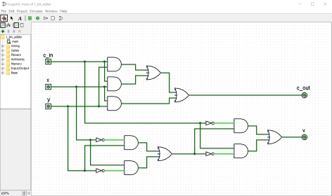
Now it's time to draw our circuit

We can also try to simulate our circuits - a good choice is a Logisim application (download Logisim project
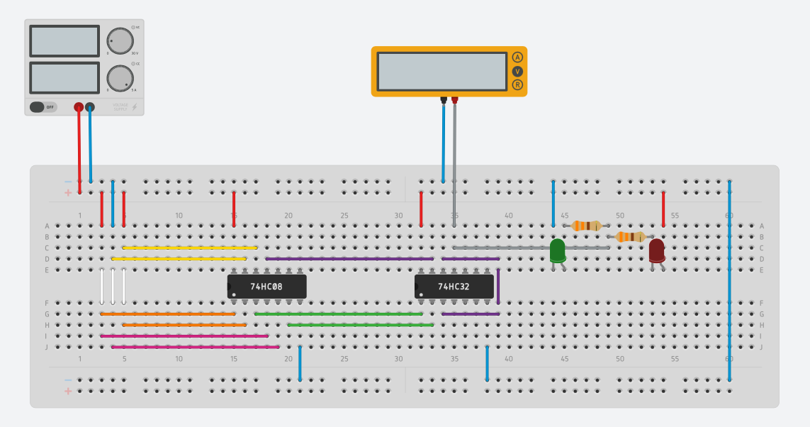
Finally you can use real components to create this circuit.
Circuit for carry signal is presented below:

|
|
Below you can see a tests for some combinations of input signals:

|
| Test for: carry_in=1, x=0, y=1, GREEN led is ON. |

|
| Test for: carry_in=0, x=1, y=0, RED led is ON. |
Full circuti is presented below:

|
| c_in = green cable, y = orange cable, x = white cable |
Above axample was completed in Autodesk Tinkercad.
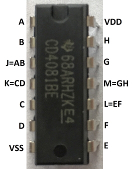
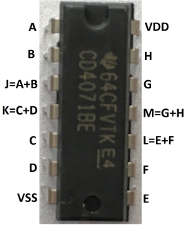
We will use the following chips with logic gates
| AND | OR | NOT |
|---|---|---|
 |
 |
 |
| CD4081BE datasheet |
CD4071BE datasheet |
CD4049 datasheet |
We can't...
- Don't touch chip's pins! Avoid electrostatic discharges to prevent chip to be damaged.
- There can be no floating inputs! All input pins must always be connect with a known voltage. This includes the input pins of gates that are unused on a chip.
- Be careful when using the output from a logic chip to power something, for example an LED. In most cases we should use transistors.
- Don’t tie the outputs together from two or more logic gates.
We can...
- We can connect the input of a gate directly to a regulated power supply, either positive side or negative side.
- We can connect the output from one gate directly to the input of another gate.
- The output from one gate can power the inputs of several other gates. The exact number depends on the chip, but with safety margin we can assume that we can power at least ten inputs with one logic output.
- Negative voltage pin is denoted as one of $VSS$, $V_{SS}$, $VEE$, $V_{EE}$, $GND$
- Positive voltage pin is denoted as one of $VDD$, $V_{DD}$, $VCC$, $V_{CC}$, $V+$
More information about adders you can find in this great article Binary Adder
Use Tinkercad to design magnitude comparator. Please, try to make it on your own. The following images may help you, if you stuck.

|

|
| Test for: x=0, y=1. |

|
| Test for: x=0, y=1. |

|
| Test for: x=1, y=0. |

|
| Test for: x=1, y=1. |
Build a 4-bit adder (logic circuit which allows to add two 4-bit numbers).